Plasma Solution Etching
Etching process
: The process of leaving only the necessary parts of the pattern of the circuit and cutting out the unnecessary parts
A-Si / poly-Si / SiO2 / Si/SiO2-selective etching / SiON / Si3N4 / PAC / MoTi
Etching exhibition
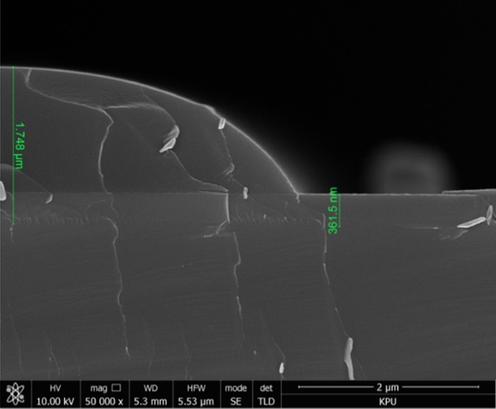
After etching
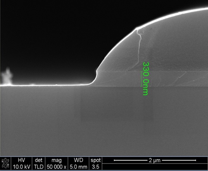
Si3N4 layor on C-wafer
Etching exhibition
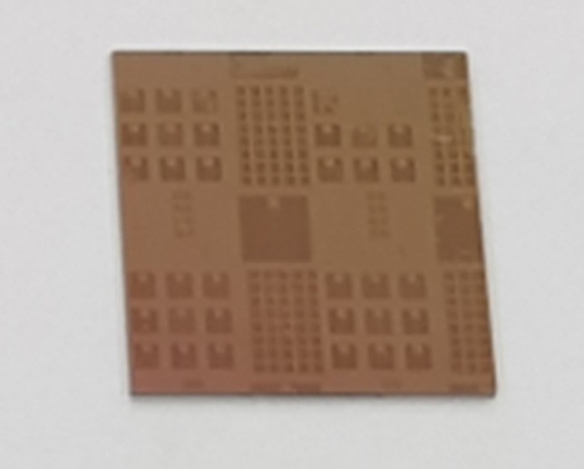
After etching
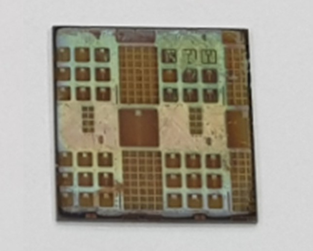
Plasma Solution Ashing
Ashing process :You don’t need any more after the photo lithography pr when stripping.
Etching exhibition
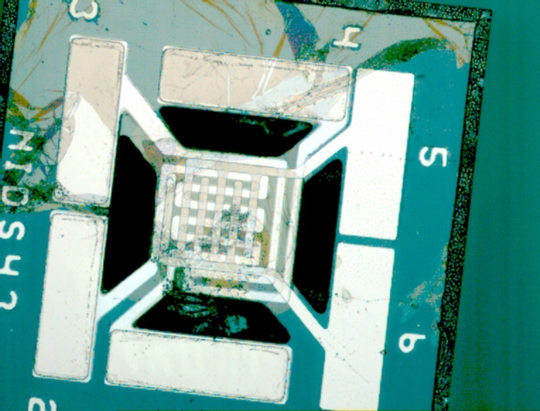
After etching
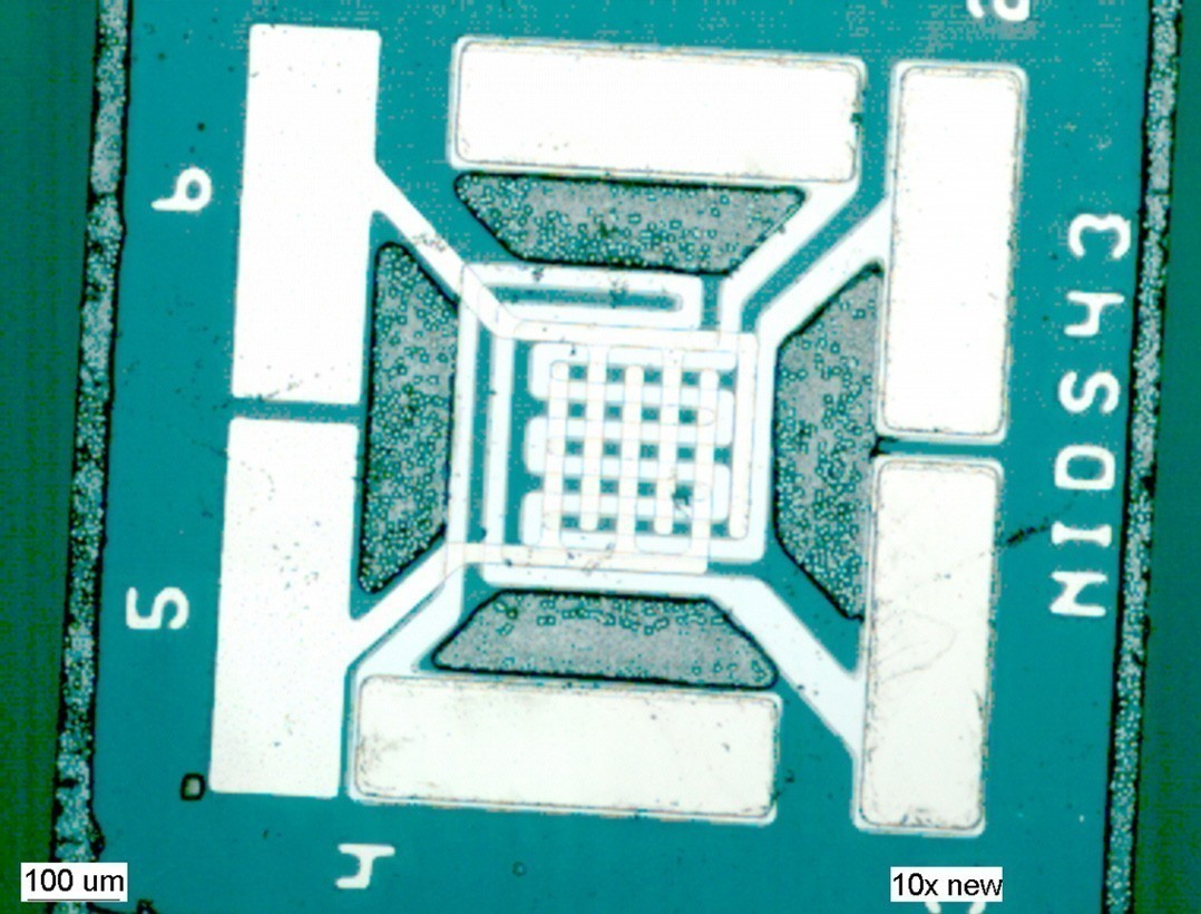
-Residue removal of polymer that has not been removed after acetone treatment
Sample size: device size: 1mm*1mm (200개), design rule: 30㎛
에칭전
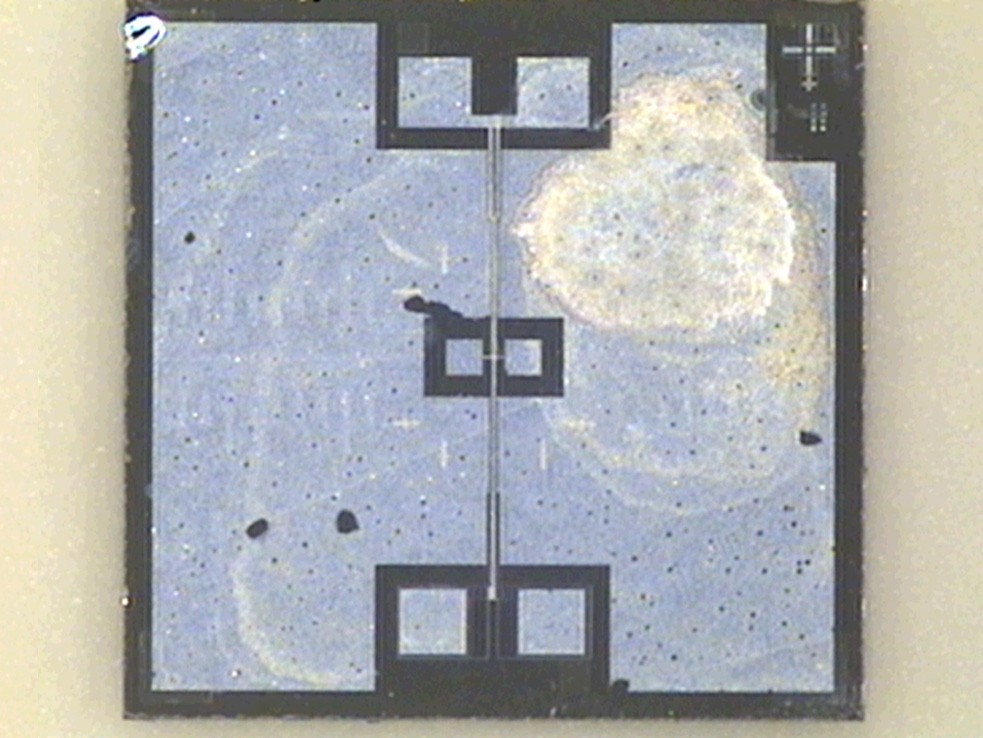
에칭후
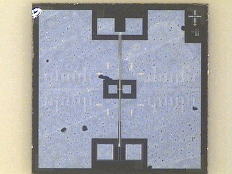
Residue removal of polymer that has not been removed after acetone treatment
Sample size: device size: 3mm*3mm , design rule:1㎛

